
Near Field Optical Microscopy
Introduction :
It is well known that optical instruments are limited by diffraction,
this limit was originally determined by E. Abbe, it is only ~ l/2 or 200
nm for visible light (l is the wavelength of light). After the achievement
of the Scanning Tunneling Microscope (STM) by G.Binnig and H.Rohrer in
1982, various form of scanning probe microscopy have been developed. The
necessity to characterize materials using optical methods at sub-micronic
scale with more precision is the motivation to combine optical microscopy
with high resolution scanning probe methods, the "Abbe barrier" was completely
broken by the resulting technique: the Scanning Near-field
Optical Microscopy (SNOM). During the last decade, SNOM, using
various configurations, in the visible region of the electromagnetic spectrum
have demonstrated very high optical resolution. Most of the time the sub-wavelength
resolution is achieved by sending or collecting the light trough a small
aperture in opaque screen. In our laboratory, we have developed another
idea. Instead of using a small aperture in metallic screen, we have used
an apertureless metallic tip which have proven
to be efficient in terms of resolution.
New results and previous studies :
| 1 IN
THE IR DOMAIN, we have obtain very good résolution on gold surface.
2 METALLIC
NANOSTRUCTURES, new set-ups allow us to study the interaction of electromagnetic
wave with such structures..
3 the ability of our SNOM to reveal polarization
contrast is used on magneto-optical samples |
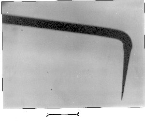
Tip's photography, the line is 500 microns long. |
.
Team
Jean Claude Rivoal, Professor
at université P. et M. Curie, Paris, France.
Lionel Aigouy, Permanent
Researcher, CNRS, France.
Gianni Carbone, PhD Student, Italy
Sebastien Ducourtieux,
PhD Student, France
Samuel Grésillon,
PhD student, France
Ahmed Lahrech, PhD student,
Moroco
Bruno Zappone, PhD Student, Italy
Contact information Jean Claude
Rivoal
Retour à la page principale / Return
to the top